PWB Corporation |
Design of PCB for electronics appliances was our beginning. |
 |
|
PCB Design/Fab/Assy >> PCB Design
▼ Advantage for PCB Design ▼ Design technology with Transmission Line Analysis and Tool for suppressing EMI ▼ PCB is now considered to be a highly functional module component. ▼ CAM data optimized for manufacturing Advantage for PCB Design
■ 40 PCB Designers
■ Transmission Line Analysis, EMI Simulation ■ High speed digital circuit design include differential pair 28Gbps, PCI-Express, DDR3-SDRAM, USB3.0, MIPI, HDMI etc ■ High density design for laptop computers, Tablet and Portable devices ■ Reduced design cycle by Auto-router, group design, different shifts, and around-the-clock design utilizing time difference between Japan and US. Design technology with Transmission Line Analysis and EMI Simulation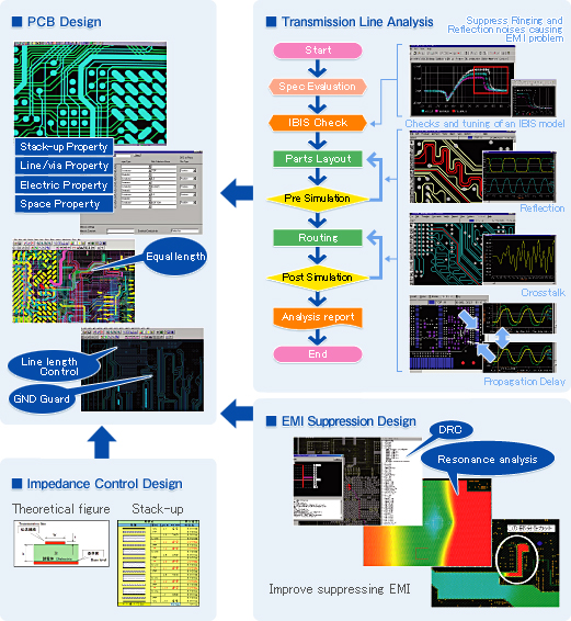
PCB is now considered to be a highly functional module component.
Timely verification and consistency by close cooperation of design, manufacturing, and assembly are the keys to producing advanced products.
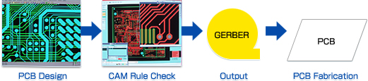
CAM data optimized for manufacturing
Manufacturing check for every article
|
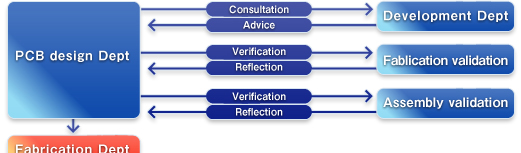
 Perform various verification prior to or during the design stage for advanced products.
| Copyright(c)2001 PWB Corporation. All rights reserved. |