Service
PCB manufacturing features
We can handle short prototype lead times, from small-lot production to large-lot mass production.
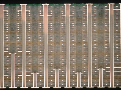
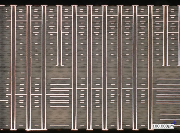
We manufacture high-density boards by combining small-diameter VIA microfabrication using high-precision drill machines and a dedicated high-aspect copper plating line with resin filling for PAD ON VIA formation and direct imaging etching control.
We can also freely combine various VIA construction methods using BVH/IVH/SVH and small-diameter through-hole VIAs, and we can achieve large, thick boards with high multi-layer construction through layering control.
Board manufacturing ability
| Size | 590×490mm |
| Thickness | 6.35t |
| Number of layers | Double-sided, 4 to 68 layers |
| Aspect | 32 |
| DUT pitch | 0.2 |
| Material | General FR-4, halogen-free, high Tg, low transmission loss |
| Zo control | 50Ω±5% |
CAM manufacturing analysis
We perform CAM manufacturing analysis on all designs, including our own and those of other companies, before manufacturing the boards.
We analyze specifications, such as the density and difficulty of the design data, and calculate the optimal manufacturing conditions for each product, enabling us to realize advanced products.
Various support cases
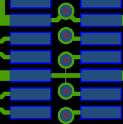
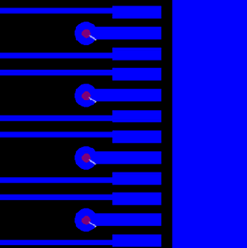
| Back drilling | Removal of plated stubs in through-holes of high-speed signal lines |
| High aspect ratio | Compatible with thick and high-density boards |
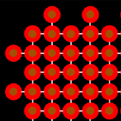
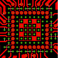
| Multi-stage BVH, SVH | Compatible with multi-pin/narrow-pitch CSP, compatible with high speed and high frequency |
| High-frequency board manufacturing | Special substrate, low transmission loss, cavity processing |
| Reliable board manufacturing | High Tg |